- 您现在的位置:买卖IC网 > Sheet目录2008 > MAX1202AEPP+ (Maxim Integrated Products)IC ADC 12BIT 8CH 20-DIP
MAX1202/MAX1203
5V, 8-Channel, Serial, 12-Bit ADCs
with 3V Digital Interface
______________________________________________________________________________________
15
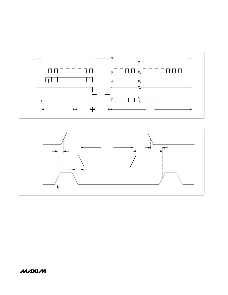
Figure 9. Internal Clock Mode Timing
SSTRB
CS
SCLK
DIN
DOUT
14
8
12
18
20
24
START
SEL2 SEL1 SEL0
UNI/
BIP
SGL/
DIF
PD1
PD0
B11
MSB
B10
B9
B2
B1
B0
LSB
ACQUISITION
1.5s
(SCLK = 2MHz)
IDLE
FILLED WITH
ZEROS
IDLE
CONVERSION
10s MAX
ADC STATE
2
3
5
6
7
9
10
11
19
21
22
23
tCONV
Figure 10. Internal Clock Mode SSTRB Detailed Timing
PD0 CLOCK IN
tSSTRB
tCSH
tCONV
tSCK
SSTRB
SCLK
tCSS
NOTE: KEEP SCLK LOW DURING CONVERSION FOR BEST NOISE PERFORMANCE.
CS
conversion is started. Pulling CS high prevents data from
being clocked into the MAX1202/MAX1203 and three-
states DOUT, but it does not adversely affect an internal
clock mode conversion already in progress. When
internal clock mode is selected, SSTRB does not go into
a high-impedance state when CS goes high.
Figure 10 shows SSTRB timing in internal clock mode.
Data can be shifted in and out of the MAX1202/MAX1203
at clock rates up to 2.0MHz, if tACQ is kept above 1.5s.
Data Framing
CS’s falling edge does not start a conversion on the
MAX1202/MAX1203. The first logic high clocked into DIN
is interpreted as a start bit and defines the first bit of the
control byte. A conversion starts on SCLK’s falling edge
after the eighth bit of the control byte (the PD0 bit) is
clocked into DIN. The start bit is defined as one of the
following:
The first high bit clocked into DIN with CS low any-
time the converter is idle (e.g., after VDD is applied).
or
The first high bit clocked into DIN after bit 5 (B5) of a
conversion in progress appears at DOUT.
If a falling edge on CS forces a start bit before B5
becomes available, the current conversion is termi-
nated and a new one started. Thus, the fastest the
MAX1202/MAX1203 can run is 15 clocks/conversion.
发布紧急采购,3分钟左右您将得到回复。
相关PDF资料
MAX121EAP+
IC ADC 14BIT 308KSPS 20SSOP
MAX1238MEEE+T
IC ADC 12BIT SERIAL 16-QSOP
MAX1240AEPA+
IC ADC 12BIT SERIAL 8-DIP
MAX1245BCPP
IC ADC SRL 12BIT 2.375V 20-DIP
MAX1249AEPE+
IC ADC 10BIT SERIAL 16-DIP
MAX1279AETC+
IC ADC 12BIT 1.5MSPS 12-TQFN
MAX1285BESA+T
IC ADC 12BIT 300KSPS 8-SOIC
MAX1302BEUG+
IC ADC 16BIT SRL 115KSPS 24TSSOP
相关代理商/技术参数
MAX1202BC/D
功能描述:模数转换器 - ADC RoHS:否 制造商:Texas Instruments 通道数量:2 结构:Sigma-Delta 转换速率:125 SPs to 8 KSPs 分辨率:24 bit 输入类型:Differential 信噪比:107 dB 接口类型:SPI 工作电源电压:1.7 V to 3.6 V, 2.7 V to 5.25 V 最大工作温度:+ 85 C 安装风格:SMD/SMT 封装 / 箱体:VQFN-32
MAX1202BCAP
功能描述:模数转换器 - ADC Integrated Circuits (ICs) RoHS:否 制造商:Texas Instruments 通道数量:2 结构:Sigma-Delta 转换速率:125 SPs to 8 KSPs 分辨率:24 bit 输入类型:Differential 信噪比:107 dB 接口类型:SPI 工作电源电压:1.7 V to 3.6 V, 2.7 V to 5.25 V 最大工作温度:+ 85 C 安装风格:SMD/SMT 封装 / 箱体:VQFN-32
MAX1202BCAP+
功能描述:模数转换器 - ADC 12-Bit 8Ch 133ksps 5V Precision ADC RoHS:否 制造商:Texas Instruments 通道数量:2 结构:Sigma-Delta 转换速率:125 SPs to 8 KSPs 分辨率:24 bit 输入类型:Differential 信噪比:107 dB 接口类型:SPI 工作电源电压:1.7 V to 3.6 V, 2.7 V to 5.25 V 最大工作温度:+ 85 C 安装风格:SMD/SMT 封装 / 箱体:VQFN-32
MAX1202BCAP+T
功能描述:模数转换器 - ADC 12-Bit 8Ch 133ksps 5V Precision ADC RoHS:否 制造商:Texas Instruments 通道数量:2 结构:Sigma-Delta 转换速率:125 SPs to 8 KSPs 分辨率:24 bit 输入类型:Differential 信噪比:107 dB 接口类型:SPI 工作电源电压:1.7 V to 3.6 V, 2.7 V to 5.25 V 最大工作温度:+ 85 C 安装风格:SMD/SMT 封装 / 箱体:VQFN-32
MAX1202BCAP-T
功能描述:模数转换器 - ADC RoHS:否 制造商:Texas Instruments 通道数量:2 结构:Sigma-Delta 转换速率:125 SPs to 8 KSPs 分辨率:24 bit 输入类型:Differential 信噪比:107 dB 接口类型:SPI 工作电源电压:1.7 V to 3.6 V, 2.7 V to 5.25 V 最大工作温度:+ 85 C 安装风格:SMD/SMT 封装 / 箱体:VQFN-32
MAX1202BCPP
功能描述:模数转换器 - ADC RoHS:否 制造商:Texas Instruments 通道数量:2 结构:Sigma-Delta 转换速率:125 SPs to 8 KSPs 分辨率:24 bit 输入类型:Differential 信噪比:107 dB 接口类型:SPI 工作电源电压:1.7 V to 3.6 V, 2.7 V to 5.25 V 最大工作温度:+ 85 C 安装风格:SMD/SMT 封装 / 箱体:VQFN-32
MAX1202BCPP+
功能描述:模数转换器 - ADC 12-Bit 8Ch 133ksps 5V Precision ADC RoHS:否 制造商:Texas Instruments 通道数量:2 结构:Sigma-Delta 转换速率:125 SPs to 8 KSPs 分辨率:24 bit 输入类型:Differential 信噪比:107 dB 接口类型:SPI 工作电源电压:1.7 V to 3.6 V, 2.7 V to 5.25 V 最大工作温度:+ 85 C 安装风格:SMD/SMT 封装 / 箱体:VQFN-32
MAX1202BEAP
功能描述:模数转换器 - ADC RoHS:否 制造商:Texas Instruments 通道数量:2 结构:Sigma-Delta 转换速率:125 SPs to 8 KSPs 分辨率:24 bit 输入类型:Differential 信噪比:107 dB 接口类型:SPI 工作电源电压:1.7 V to 3.6 V, 2.7 V to 5.25 V 最大工作温度:+ 85 C 安装风格:SMD/SMT 封装 / 箱体:VQFN-32